Home » Working Principle » Pure Sine Wave Inverter Working Principle
Pure Sine Wave Inverter Working Principle
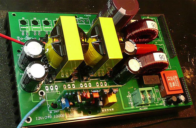
Pure Sine Wave Inverter (see image) is majority organized by MOS field effect transistor and normal power transformer. The output power depends on the MOS field effect transistor and power transformer. It is suitable for amateur makings of electron fans, for it can avoid complex transformer winding. The following article will introduce you about the working principle and making process of the inverter.

Pure Sine Wave Inverter Working principle
Now we will detailed introduce the working principle of the sine wave power inverter.
Square signal generator (see image 2)
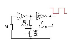
The square signal generator of the inverter applied hex inverter CD4069. R1 in the circuit is the compensation resistance, used to balance the oscillation frequency of power voltage vibration. Circuital vibration is caused by charge-discharge of capacitance C1. The vibration frequency is f=1/2.2RC. The maximum frequency of the inverter circuit in image is: fmax=1/2.2×3.3×103×2.2×10-6=62.6Hz; Minimum frequency is: fmin=1/2.2×4.3×103×2.2×10-6=48.0Hz. The reality value may have slightly difference for component error. Ground connect the input ends other inverter to avoid affection.
Field effect transistor driving circuit

Image 3
For the maximum amplitude of the output vibration signal voltage of the square signal generator is 0-5V. To ensure full driving of power switch circuit, we applied TR1, TR2 to magnify the vibration signal voltage to 0-12V. Refer to image 3.
MOS field effect transistor power switching circuit is the core of the inverter device. Before introducing the working principle of the part, we will introduce about the MOS field effect transistor for the power inverter.

Image 4
MOS field effect transistor is also called MOS FET (Metal Oxide Semiconductor Field Effect Transistor). It has two types of depletion and enhancement. We use the enhancement type MOS FET (interior structure refer to image 4) for the pure sine wave inverter. It can be divided in to NPN type and PNP type. NPN type is often called N channel type; PNP type is often called P channel type. We can know from the image that the source and drain electrodes of N channel field effect transistor are installed on N type semiconductor, while P channel type is installed on P type semiconductor. We all know that the output current is controlled by input current in dynatron. But for field effect transistor, the output current is controlled by input voltage. We consider the input current to be extremely low or there is no input current. The device has very high input resistance for this, and this is the reason we call it as field effect transistor.

Image 5
To explain the working principle of MOS field effect transistor, we should know the working principle of a diode with only one P-N knot. In image 5, we know that the diode will have current flow when plus with forward voltage (P side connect with positive pole, N connect with negative pole). This is because when the P type semiconductor is under positive voltage, the negative electron of N type semiconductor will flow to P type side, while the positive electron of P type flowing to N type, which forms the break over current. Similarly, when the diode is under backward voltage, the positive electron will gather in P type, while negative electron gather in N type, all the electron will not move with no current to be flow, the diode will be cut-off.

As for true sine wave inverter applied field effect transistor (image 6), we can know from the analysis above that there will be no current flow between source electrode and drain electrode, the field effect transistor is under cut-off situation (image 6a). When a positive voltage is added to N channel MOS field effect transistor grid, the electron will gather in the N channel P type semiconductor because of the resist of oxidation film (image 6b), the source and drain electrode will be connected with current. We can imagine that there is a gap between the two N type semiconductors, building the grid voltage is to build a bridge for them, the size the bridge is decided by the grid. Image 7 shows the working procedure of P channel MOS field effect transistor, the detailed working principle is similar so it will not be repeated.

Image 7
Now we introduce about the working procedure of C-MOS field effect transistor organized inverter application circuit (image 8). The circuit combined an enhanced P channel MOS field effect transistor and an enhanced N channel field effect transistor. When the input side is under low electrical level, P channel field effect transistor connect, the output side connect with power supply. In the circuit, the P channel and N channel field effect transistor always work under opposite condition, the phase position input and output side is in opposite position. Under such working mode, we can get higher current output. At the same time, for the effect of leaking current, the MOS field effect transistor will be shut down when the grid current is lower than 1-2V. Different field effect transistor has different turn-off current. Just because of this, the circuit will not be shorted out when connect both field effect transistors.

Image 8
From the analysis above we can draw out the working procedure of MOS field effect transistor circuit part (image 9). The pure sine wave inverter working principle is mentioned above. When the alternate signal with low voltage, high current and 50Hz frequency pass through low voltage winding of the transformer, it will introduce high alternating voltage to complete the shifting of DC to AC. It should be notice that, in some conditions, such as when the vibration part stop working, the low voltage side of the transformer will have large current, so, the fuse of the circuit should not be removed or shorted.

Image 9
Key points of utilizing
Circuit board refers to image 10. Components and parts refer to image 11. The transformer for the inverter applies 12V secondary voltage, 10A current, and 220V primary voltage made-up power transformer. P channel MOS field effect transistor (2SJ471) has a maximum drain current of 30A. When the field effect transistor is connected, resistance between source-drain electrodes is 25 milliohm. At this time, 10A current flow will have 2.5W power consumption. N channel MOS field effect transistor (2SK2956) has maximum current of 50A. When the field effect transistor is connected, resistance between source-drain electrodes is 7 milliohm. At this time, 10A current flow will have 0.7W power consumption. So, we can know that 2SJ471 will have 4 times calorific value than 2SK2957 under same current. We should pay attention to this when consider about radiator. Image 12 shows the position distribution and connection of the mentioned field effect transistor in radiator (100mm×100mm×17mm). Although the field effect transistor will not be too hot under on-off state, we still choose larger radiator for security consideration.

Image 10

Image 11

Image 12
Performance testing of pure sine wave inverter
Testing inverter circuit refers to image 13. The testing apply 12V automobile battery with low internal resistance and large discharging current (larger than 100A) to offer plenty input power. The testing media is a normal bulb. Testing method is to change the loading capacity and measure the input current, voltage and output current. The testing result refers to image 14a. We can see that, output voltage will reduce when the load increases, power consumption of the bulb will also change will voltage. We can find the relationship of voltage and power. But in fact, the resistance of the bulb may change, the output voltage and current are not sine wave, so the calculating is only estimation. According to the example of 60W electric bulb:
Assume that the resistance of bulb will not change with voltage. For R bulb=V2/W=2102/60=735Ω, so when voltage=208V, W=V2/R=2082/735=58.9W. We can convert the relationship of voltage and power. By testing, we found that when the output power is about 100W, input current is 10A. At this time, output voltage is 200V. Power efficiency of field effect transistor refers to image 14b. Image 15 is the temperature rise graph of the field effect transistor under 100W loading. Image 16 is the output wave graph of different loading. The graphs are only for reference.

Image 13

Image 14

Image 15 & 16
Pure Sine Wave Inverter Working principle
Now we will detailed introduce the working principle of the sine wave power inverter.
Square signal generator (see image 2)
The square signal generator of the inverter applied hex inverter CD4069. R1 in the circuit is the compensation resistance, used to balance the oscillation frequency of power voltage vibration. Circuital vibration is caused by charge-discharge of capacitance C1. The vibration frequency is f=1/2.2RC. The maximum frequency of the inverter circuit in image is: fmax=1/2.2×3.3×103×2.2×10-6=62.6Hz; Minimum frequency is: fmin=1/2.2×4.3×103×2.2×10-6=48.0Hz. The reality value may have slightly difference for component error. Ground connect the input ends other inverter to avoid affection.
Field effect transistor driving circuit
Image 3
For the maximum amplitude of the output vibration signal voltage of the square signal generator is 0-5V. To ensure full driving of power switch circuit, we applied TR1, TR2 to magnify the vibration signal voltage to 0-12V. Refer to image 3.
MOS field effect transistor power switching circuit is the core of the inverter device. Before introducing the working principle of the part, we will introduce about the MOS field effect transistor for the power inverter.
Image 4
MOS field effect transistor is also called MOS FET (Metal Oxide Semiconductor Field Effect Transistor). It has two types of depletion and enhancement. We use the enhancement type MOS FET (interior structure refer to image 4) for the pure sine wave inverter. It can be divided in to NPN type and PNP type. NPN type is often called N channel type; PNP type is often called P channel type. We can know from the image that the source and drain electrodes of N channel field effect transistor are installed on N type semiconductor, while P channel type is installed on P type semiconductor. We all know that the output current is controlled by input current in dynatron. But for field effect transistor, the output current is controlled by input voltage. We consider the input current to be extremely low or there is no input current. The device has very high input resistance for this, and this is the reason we call it as field effect transistor.
Image 5
To explain the working principle of MOS field effect transistor, we should know the working principle of a diode with only one P-N knot. In image 5, we know that the diode will have current flow when plus with forward voltage (P side connect with positive pole, N connect with negative pole). This is because when the P type semiconductor is under positive voltage, the negative electron of N type semiconductor will flow to P type side, while the positive electron of P type flowing to N type, which forms the break over current. Similarly, when the diode is under backward voltage, the positive electron will gather in P type, while negative electron gather in N type, all the electron will not move with no current to be flow, the diode will be cut-off.
| Image 6a | Image 6b |
As for true sine wave inverter applied field effect transistor (image 6), we can know from the analysis above that there will be no current flow between source electrode and drain electrode, the field effect transistor is under cut-off situation (image 6a). When a positive voltage is added to N channel MOS field effect transistor grid, the electron will gather in the N channel P type semiconductor because of the resist of oxidation film (image 6b), the source and drain electrode will be connected with current. We can imagine that there is a gap between the two N type semiconductors, building the grid voltage is to build a bridge for them, the size the bridge is decided by the grid. Image 7 shows the working procedure of P channel MOS field effect transistor, the detailed working principle is similar so it will not be repeated.
Image 7
Now we introduce about the working procedure of C-MOS field effect transistor organized inverter application circuit (image 8). The circuit combined an enhanced P channel MOS field effect transistor and an enhanced N channel field effect transistor. When the input side is under low electrical level, P channel field effect transistor connect, the output side connect with power supply. In the circuit, the P channel and N channel field effect transistor always work under opposite condition, the phase position input and output side is in opposite position. Under such working mode, we can get higher current output. At the same time, for the effect of leaking current, the MOS field effect transistor will be shut down when the grid current is lower than 1-2V. Different field effect transistor has different turn-off current. Just because of this, the circuit will not be shorted out when connect both field effect transistors.
Image 8
From the analysis above we can draw out the working procedure of MOS field effect transistor circuit part (image 9). The pure sine wave inverter working principle is mentioned above. When the alternate signal with low voltage, high current and 50Hz frequency pass through low voltage winding of the transformer, it will introduce high alternating voltage to complete the shifting of DC to AC. It should be notice that, in some conditions, such as when the vibration part stop working, the low voltage side of the transformer will have large current, so, the fuse of the circuit should not be removed or shorted.
Image 9
Key points of utilizing
Circuit board refers to image 10. Components and parts refer to image 11. The transformer for the inverter applies 12V secondary voltage, 10A current, and 220V primary voltage made-up power transformer. P channel MOS field effect transistor (2SJ471) has a maximum drain current of 30A. When the field effect transistor is connected, resistance between source-drain electrodes is 25 milliohm. At this time, 10A current flow will have 2.5W power consumption. N channel MOS field effect transistor (2SK2956) has maximum current of 50A. When the field effect transistor is connected, resistance between source-drain electrodes is 7 milliohm. At this time, 10A current flow will have 0.7W power consumption. So, we can know that 2SJ471 will have 4 times calorific value than 2SK2957 under same current. We should pay attention to this when consider about radiator. Image 12 shows the position distribution and connection of the mentioned field effect transistor in radiator (100mm×100mm×17mm). Although the field effect transistor will not be too hot under on-off state, we still choose larger radiator for security consideration.
Image 10
Image 11
Image 12
Performance testing of pure sine wave inverter
Testing inverter circuit refers to image 13. The testing apply 12V automobile battery with low internal resistance and large discharging current (larger than 100A) to offer plenty input power. The testing media is a normal bulb. Testing method is to change the loading capacity and measure the input current, voltage and output current. The testing result refers to image 14a. We can see that, output voltage will reduce when the load increases, power consumption of the bulb will also change will voltage. We can find the relationship of voltage and power. But in fact, the resistance of the bulb may change, the output voltage and current are not sine wave, so the calculating is only estimation. According to the example of 60W electric bulb:
Assume that the resistance of bulb will not change with voltage. For R bulb=V2/W=2102/60=735Ω, so when voltage=208V, W=V2/R=2082/735=58.9W. We can convert the relationship of voltage and power. By testing, we found that when the output power is about 100W, input current is 10A. At this time, output voltage is 200V. Power efficiency of field effect transistor refers to image 14b. Image 15 is the temperature rise graph of the field effect transistor under 100W loading. Image 16 is the output wave graph of different loading. The graphs are only for reference.
Image 13
Image 14
Image 15 & 16
From the circuit and the output waveforms shown this is a square, not sine, wave inverter. Am I right?
Post a Comment:
You may also like:

Power Inverter Source
Featured Articles
How to Choose a Suitable Power ...
 How to select the inverter for an air conditioner, television, computer or the motor? How to match the battery? How long is the ...
How to select the inverter for an air conditioner, television, computer or the motor? How to match the battery? How long is the ...12V 300W Uni-polar Isolation Pure Sine ...
 12v 300w uni-polar isolation of pure sine wave inverter Basic parameters Nominal power: 300W; continuous power: 250W; Peak power: ...
12v 300w uni-polar isolation of pure sine wave inverter Basic parameters Nominal power: 300W; continuous power: 250W; Peak power: ...600w Pure Sine Wave Power Inverter ...
 I spent nearly a month design a 600w pure sine wave power inverter. The machine has the following characteristics: 1. SPWM drive ...
I spent nearly a month design a 600w pure sine wave power inverter. The machine has the following characteristics: 1. SPWM drive ...1000w 12V DC Home Power Inverter ...
 This power inverter is designed for 12v DC, but also can be connected to 24v DC, my goal is 800 watt, strive to 1000 watt pure ...
This power inverter is designed for 12v DC, but also can be connected to 24v DC, my goal is 800 watt, strive to 1000 watt pure ...