12V 300W Uni-polar Isolation Pure Sine Wave Inverter Design
I. 12v 300w uni-polar isolation of pure sine wave inverter Basic parameters
Nominal power: 300W; continuous power: 250W; Peak power: 600W;
Output voltage: Output single phase 220VAC (RMS), a frequency of 50±1Hz.
Overall efficiency: 87%; 300 times the power short-circuit, short-circuit power 200 times;
Overload protection 500W; immediate short circuit protection; voltage alarm 10.3V delay 1.5S;
Under-voltage protection 10V immediate shutdown; over-voltage protection 15V immediate shutdown; overheat protection: 65℃.
II. Framework and composition
Overall, this is a uni-polar 12V isolating pure sine wave inverter. This inverter is composed of three parts: pre-driver board, stage driver board and power board.
1. The pre-driver board is mainly composed by three parts: the power supply section, PWM driving portion and over-voltage protection section;
2. The stage driver board is composed of three parts: generating (SCM EG8010) SPWM signal portion, the driving portion of the IR2110, and over-current protection section. (See Detailed EG8010 SPWM chip data sheet);
3. Power board main components: the power board includes a pre-reverse polarity protection, DC-DC step-up push-pull, H-bridge inverter and rectifier filter section; also includes over-current protection circuit, a quasi-closed loop feedback section and under small portion of voltage alarm circuit.
III. 12v 300w inverter circuit structure and principle analysis
1. Pre-amp driver board
A. power supply part
In the first stage driver circuit, BT input voltage range of 10-15V, and SG3525 wide operating voltage range of 8-35V, LM358 single supply voltage range of 3-30V, so BT voltage sufficient to drive the two chips, so the first stage power supply may be used as part of BT powered.
B. PWM driving part

As shown above, the PWM signal generating circuit SG3525, when this part of the circuit's access to power 12V, SG3525 was electric, and then set up by the internal oscillator and external oscillator capacitor C4, a resistor R5 and the dead time of oscillation resistor R8 constitute Dr tooth wave generating circuit, provides the clock source for the entire IC, so that the IC work states, because access to the boot soft-start capacitor C6. Power output rectangular pulse after the change is to start with the minimum duty cycle to 50% of the state, mainly to protect the signal is not being driven by a power MOS step in a larger duty cycle of state, to reduce the power of the moment MOS impact pressure.
SG3525 chip, the PWM signal generated by 11 feet and 14 feet, and the feet output, the output waveform phase difference of 180 degrees, are out of phase. Note that the figure above there are two 10K resistors (R10 and R11) PWM signal PWM1 and PWM2 pulled in two signals, what use is it, in fact, this drop is necessary, is to increase the SG3525 PWM signal a dummy load, so that the signal is not stable floating jump. Not because of some static electricity generated during off high, the MOS gate of the power board while generating a high level, in the high-capacity battery power is turned on while the bombing. SG3525 pin map as follows (see SG3525 More Detailed Information):

1. Inv.input (Pin 1): Error amplifier inverting input.
2. Noninv.input (Pin 2): Error Amplifier with input terminal.
3. Sync (Pin 3): External oscillator sync signal input.
4. OSC.Output (Pin 4): Oscillator output.
5. CT (Pin 5): Oscillator timing capacitor terminal access.
6. RT (Pin 6): Oscillator timing resistor access points.
7. Discharge (Pin 7): Oscillator discharge end.
8. Soft-Start (Pin 8): Soft-start capacitor access points.
9. Compensation (Pin 9): PWM comparator compensation signal input terminal.
10. Shutdown (Pin 10): Off-signal external input terminal.
11. Output A (Pin 11): Output A.
12. Ground (pin 12): Signal ground.
13. Vc (Pin 13): Output stage bias voltage terminal access.
14. Output B (Pin 14): Output B. Pin 14 and pin 11 are two complementary outputs.
15. Vcc (Pin 15): Bias supply terminal access.
16. Vref (pin 16): Reference power output.
In this 12v 300 watt inverter circuit, the voltage feedback SG3525 uses quasi-closed loop modulation. The principle is, + 5V through R9 and R4 partial pressure is provided by a 16-foot SG3525 generated SG3525 2 feet to the introduction of a fixed reference voltage, high-voltage component HV 1 foot before the next stage boosted, when the output of high voltage components when HV fixed value greater than 2 feet, of SG3525 internal error amplifier 2 will be greater than the variable voltage pin as an error, it amplifies the error amplified to modulate the amount of the duty ratio of PWM, the inverter there is a small stream static load at boot time. This feature is good in principle. Enable the PWM duty cycle at no load to a minimum, at the time of the tape should be immediately pulled the maximum duty cycle, using a circuit work at the highest efficiency state.
C. Over voltage and under voltage protection section

As it shown above, the protection part of the circuit by the LM358 is completed. The protection circuit is a simple window comparator circuit includes only the over-voltage and under-voltage protection. Working principle is as follows: Because the BT input voltage range of 10-15V, while BT is lower than 10V voltage, high voltage 15V when BT as over-voltage, under-voltage so set USW = 10V when, U1 reference point for the under-voltage protection, when USW=15V when over-voltage, U2 reference point for the over-voltage protection. As shown above by the +5V power supply, R7, R14, R22 set the comparator reference voltage U1, U2.
Under-voltage protection: When the SW terminal voltage USW≦10V, LM358 voltage Usw1 6 feet will be lower than 5 feet U1,7 feet high output voltage, namely SD control pin is high, the SG3525 10-foot control SD feet high, so that the shutdown of the PWM signal output.
Over-voltage protection: When SW terminal voltage USW≧15V, LM358 3 feet voltage Usw2 will be higher than 2 feet U1,7 feet high output voltage, namely SD control pin is high, the SG3525 10-foot control SD feet high, so that the shutdown of the PWM signal output.
Note: As the chart above, R20 and R21 is very important, both for the 1M resistor. Play a positive role in the feedback circuit, so LM358 constitute a hysteresis circuit. Ling effectively reduce vibration switch; adjust potentiometer R22 can change the hysteresis threshold and hysteresis size.
2. Power-amp driver board
1) Power supply section:
+5V power supply the EG8010. It needs +5V stable power supply for the rear plate. +15V power supply the IR2110S chip. The main part of the power supply after the full-wave rectified by, filter and regulator produced by the auxiliary power transformer, as shown below (the portion of the power board):

2) SPWM section:
A. SPWM generation
Mainly by single chip EG8010. (See Detailed EG8010 SPWM chip data sheet)
B. Protective section
1) Over-current detection:
Circuit reference "EG8010 SPWM chip data sheet" 6.2 EG8010 + IR2110S + Typical application circuit lockout pure sine wave inverter (unipolar modulation).
We can use RS current sampling method. The method is, after the H-bridge power stage under the S pole tube sampling resistor in series to the power ground, when there is an overload or short circuit, there will be a large current flows through the sampling resistor. When the pressure drops, use a professional comparator for comparison, the value will be greater than this output. Then, it will cite the high level to make protect shutdown signal. When the overload shutdown pre- and post-level SPWM PWM drives before and after the signal, the protection level MOS tube will not be damaged due to excessive current.
Filter the collected signal into two routes to go through R38 and C24 composed of a short latency, and then control the micro-controller EG8010 14 feet IFB, determine whether the shutdown SPWM signal. All the way to the introduction of comparative after the 3 feet LM393 device and 2 feet comparison reference voltage, then the signal from the comparator generates a foot to control two 13 foot SD IR2110S.
Because when inductive or capacitive loading, inverter power may exceed the designed overload power. But it cannot be shut-off. So, the access comparator before the signal RC (R7, C21) delay, the facilitating stable and effective inverter driven large impact load. It is similar to the image above. Circuit and overload protection way is a serious overload short-circuit protection. Overload only constant RC delay to be set after a short circuit in the post-stage H-bridge MOS does not burn in the range can be.
2) Adjusting the output voltage feedback: Since this circuit is a unipolar inverter circuit, so under unipolar modulation mode, EG8010 chip AC output voltage feedback VFB measuring 13 feet by the inverter.
As shown below: Connect post-acquisition EG8010 and 13 feet VFB port, in order to adjust the output voltage.

3) Temperature detection feedback: EG8010 chip 15 feet TFB for detecting the operating temperature of the inverter mainly used for over-temperature detection and temperature LCD action. 510Ω resistance corresponding to the selection of 25 ℃ thermistor; if you do not use temperature protection, this pin needs to be grounded.
4) Fan control:
7 feet FANCTR EG8010 chip for fan control terminal of the power supply part provided, as shown below (the portion of the power board) from the auxiliary power supply via the half-wave rectifier. When the chip 15 feet TFB pin detects a temperature when higher than 45℃, 7 feet FANCTR chip-side output and the collector of the transistor S8050 transmitter is turned on (transistor switching action). The fan will operates. When the operating temperature is lower than 40℃, the chip 7 pin output low level , the fan stops working.

5) Dead time settings: DT1 EG8010 chip 1 foot and 2 feet DT0 is controls dead time. The dead time controlling is an important parameter of power MOS transistors. If there is no dead time or it is too low, the H-bridge will be burned while conducting MOS transistor phenomenon. If it is too high, waveform distortion will lead to serious power tube heat phenomenon. See EG8010 SPWM chip data sheet pin description and select the dead time according to requirement.
C. IR2110S driving portion:
IR2110S driver circuit is a typical application circuit. You can download the circuit diagram for further analysis. (Search IR2110 for more information)
Pin map and pin names:

LO (pin 1): Low-end output.
COM (Pin 2): Common.
Vcc (pin 3): Low-end fixed supply voltage.
Nc (Pin 4): Dead-end.
Vs (Pin 5): High voltage floating supply offset.
VB (Pin 6): High-end floating power supply voltage.
HO (Pin 7): High output.
Nc (Pin 8): Dead-end.
VDD (Pin 9): Logic Supply Voltage.
HIN (Pin 10): Logic high input.
SD (Pin 11): Shutdown.
LIN (Pin 12): Logic low-end input.
Vss (Pin 13): Logic circuit ground potential terminal, and its value may be 0V.
Nc (Pin 14): Dead-end.
3. Power board portion
A. Pre-reverse polarity protection:

FET figure is IR1404 (TO-220 package) N-channel MOS transistor. MOS tube through S and D pin connected in series between the power source and the load resistor R44 = 10Ω and R13 = 10K for the MOS tube which providing a bias voltage using the switching characteristics of MOS transistors of the control circuit is turned on and off. Positive connection time, R44 provides gate voltage Vgs, MOS saturated conduction. When reverse Vgs cannot reach the threshold voltage MOS, MOS cannot be turned on, the anti-reverse play a role.
B. Power supply section
Because this circuit is isolated, it is supplied by front and rear power. So the first stage with a 78L05 (TO-92) power supply, the posterior pole with 7815 (TO-220) and 7805 (TO-220) power supply (driver power supply section See previous post). As shown in the circuit diagram:

C. DC-DC step-up push-pull, H-bridge inverter and rectifier filter section:
BT voltage of the device is 12V. At full power, pre-operating current will go up to 25A. DC-DC boost section contains a pair of IR1404 (TO-220) package power tube. Main transformer uses EI406 (vertical) core. Powered push-pull part applied the pre-symmetrical balanced method. Fast high-voltage rectifier diode use HER308. Inductive 27MM, 2.2mH magnetic ring, high-voltage filter capacitor is large capacitor 100uF/450V, and this capacitor in the circumstances permitted, as far as possible with larger capacity, to improve the load characteristics of the high-pressure part and reduce interference are good . H-bridge inverter part using four FDP18N50, voltage 500V, maximum current of 18A, the front and rear stage MOS transistor is very abundant, H-bridge circuit is part of the conventional circuit.
D. Quasi-closed loop feedback part:

Pre-voltage feedback control using optocoupler PE817 TL431 do isolation quasi closed-loop feedback circuit. After the adoption of the resistor R43 and R4 to 400V high voltage is sampled and TL431 internal reference voltage 1.25V comparing TL431 to control the turn-on and turn-off, then the voltage HV through the optocoupler control, thereby controlling the output signal pre-SG3525 role. R12, C7 and TL431 internal comparator constitute the integrator circuit.
E. Over-current protection circuit (overload protection function):

Through diode D5 and D4 respectively EI406 transformer primary current were collected before and after the comparator reference voltage, and outputs a signal SD to control pre-SG3525.
F. Under-voltage alarm circuit:

When the terminal voltage USW≦10V, the front stage will be in under-voltage condition. The comparator LM358 voltage is less than 2 feet 3 feet of the reference voltage, LM358 1 foot high, so the NE555 4 feet high, then NE555 oscillation circuit is operative to produce 1.5S drip alarm.
IV. 12v 300w uni-polar isolation of pure sine wave power inverter PCB board assembly and testing
(Note: After get the circuit diagram, weld carefully to avoid wrong welding parameters!)
Pre-amp driver board
Empty board:

Installed as shown below:

Power-amp driver board

Power Board
Empty board:

PCB:

Installed as shown below:

Then, is the testing of the over-voltage protection. This part should not be difficult, there is not much to say (in accordance with the parameters of the drawings should be no problem).
Finally, is the most important test of overload and short circuit protection, and this is the most important property for an inverter.
Everything has been basically successful commissioning, load the 12V 300W Uni-polar Isolation Pure Sine Wave Inverter for more than one hour operating, and then shut down, discharge the high-voltage.
And then install the radiator, as it shown like this:

Nominal power: 300W; continuous power: 250W; Peak power: 600W;
Output voltage: Output single phase 220VAC (RMS), a frequency of 50±1Hz.
Overall efficiency: 87%; 300 times the power short-circuit, short-circuit power 200 times;
Overload protection 500W; immediate short circuit protection; voltage alarm 10.3V delay 1.5S;
Under-voltage protection 10V immediate shutdown; over-voltage protection 15V immediate shutdown; overheat protection: 65℃.
II. Framework and composition
Overall, this is a uni-polar 12V isolating pure sine wave inverter. This inverter is composed of three parts: pre-driver board, stage driver board and power board.
1. The pre-driver board is mainly composed by three parts: the power supply section, PWM driving portion and over-voltage protection section;
2. The stage driver board is composed of three parts: generating (SCM EG8010) SPWM signal portion, the driving portion of the IR2110, and over-current protection section. (See Detailed EG8010 SPWM chip data sheet);
3. Power board main components: the power board includes a pre-reverse polarity protection, DC-DC step-up push-pull, H-bridge inverter and rectifier filter section; also includes over-current protection circuit, a quasi-closed loop feedback section and under small portion of voltage alarm circuit.
III. 12v 300w inverter circuit structure and principle analysis
1. Pre-amp driver board
A. power supply part
In the first stage driver circuit, BT input voltage range of 10-15V, and SG3525 wide operating voltage range of 8-35V, LM358 single supply voltage range of 3-30V, so BT voltage sufficient to drive the two chips, so the first stage power supply may be used as part of BT powered.
B. PWM driving part
As shown above, the PWM signal generating circuit SG3525, when this part of the circuit's access to power 12V, SG3525 was electric, and then set up by the internal oscillator and external oscillator capacitor C4, a resistor R5 and the dead time of oscillation resistor R8 constitute Dr tooth wave generating circuit, provides the clock source for the entire IC, so that the IC work states, because access to the boot soft-start capacitor C6. Power output rectangular pulse after the change is to start with the minimum duty cycle to 50% of the state, mainly to protect the signal is not being driven by a power MOS step in a larger duty cycle of state, to reduce the power of the moment MOS impact pressure.
SG3525 chip, the PWM signal generated by 11 feet and 14 feet, and the feet output, the output waveform phase difference of 180 degrees, are out of phase. Note that the figure above there are two 10K resistors (R10 and R11) PWM signal PWM1 and PWM2 pulled in two signals, what use is it, in fact, this drop is necessary, is to increase the SG3525 PWM signal a dummy load, so that the signal is not stable floating jump. Not because of some static electricity generated during off high, the MOS gate of the power board while generating a high level, in the high-capacity battery power is turned on while the bombing. SG3525 pin map as follows (see SG3525 More Detailed Information):
1. Inv.input (Pin 1): Error amplifier inverting input.
2. Noninv.input (Pin 2): Error Amplifier with input terminal.
3. Sync (Pin 3): External oscillator sync signal input.
4. OSC.Output (Pin 4): Oscillator output.
5. CT (Pin 5): Oscillator timing capacitor terminal access.
6. RT (Pin 6): Oscillator timing resistor access points.
7. Discharge (Pin 7): Oscillator discharge end.
8. Soft-Start (Pin 8): Soft-start capacitor access points.
9. Compensation (Pin 9): PWM comparator compensation signal input terminal.
10. Shutdown (Pin 10): Off-signal external input terminal.
11. Output A (Pin 11): Output A.
12. Ground (pin 12): Signal ground.
13. Vc (Pin 13): Output stage bias voltage terminal access.
14. Output B (Pin 14): Output B. Pin 14 and pin 11 are two complementary outputs.
15. Vcc (Pin 15): Bias supply terminal access.
16. Vref (pin 16): Reference power output.
In this 12v 300 watt inverter circuit, the voltage feedback SG3525 uses quasi-closed loop modulation. The principle is, + 5V through R9 and R4 partial pressure is provided by a 16-foot SG3525 generated SG3525 2 feet to the introduction of a fixed reference voltage, high-voltage component HV 1 foot before the next stage boosted, when the output of high voltage components when HV fixed value greater than 2 feet, of SG3525 internal error amplifier 2 will be greater than the variable voltage pin as an error, it amplifies the error amplified to modulate the amount of the duty ratio of PWM, the inverter there is a small stream static load at boot time. This feature is good in principle. Enable the PWM duty cycle at no load to a minimum, at the time of the tape should be immediately pulled the maximum duty cycle, using a circuit work at the highest efficiency state.
C. Over voltage and under voltage protection section
As it shown above, the protection part of the circuit by the LM358 is completed. The protection circuit is a simple window comparator circuit includes only the over-voltage and under-voltage protection. Working principle is as follows: Because the BT input voltage range of 10-15V, while BT is lower than 10V voltage, high voltage 15V when BT as over-voltage, under-voltage so set USW = 10V when, U1 reference point for the under-voltage protection, when USW=15V when over-voltage, U2 reference point for the over-voltage protection. As shown above by the +5V power supply, R7, R14, R22 set the comparator reference voltage U1, U2.
Under-voltage protection: When the SW terminal voltage USW≦10V, LM358 voltage Usw1 6 feet will be lower than 5 feet U1,7 feet high output voltage, namely SD control pin is high, the SG3525 10-foot control SD feet high, so that the shutdown of the PWM signal output.
Over-voltage protection: When SW terminal voltage USW≧15V, LM358 3 feet voltage Usw2 will be higher than 2 feet U1,7 feet high output voltage, namely SD control pin is high, the SG3525 10-foot control SD feet high, so that the shutdown of the PWM signal output.
Note: As the chart above, R20 and R21 is very important, both for the 1M resistor. Play a positive role in the feedback circuit, so LM358 constitute a hysteresis circuit. Ling effectively reduce vibration switch; adjust potentiometer R22 can change the hysteresis threshold and hysteresis size.
2. Power-amp driver board
1) Power supply section:
+5V power supply the EG8010. It needs +5V stable power supply for the rear plate. +15V power supply the IR2110S chip. The main part of the power supply after the full-wave rectified by, filter and regulator produced by the auxiliary power transformer, as shown below (the portion of the power board):
2) SPWM section:
A. SPWM generation
Mainly by single chip EG8010. (See Detailed EG8010 SPWM chip data sheet)
B. Protective section
1) Over-current detection:
Circuit reference "EG8010 SPWM chip data sheet" 6.2 EG8010 + IR2110S + Typical application circuit lockout pure sine wave inverter (unipolar modulation).
We can use RS current sampling method. The method is, after the H-bridge power stage under the S pole tube sampling resistor in series to the power ground, when there is an overload or short circuit, there will be a large current flows through the sampling resistor. When the pressure drops, use a professional comparator for comparison, the value will be greater than this output. Then, it will cite the high level to make protect shutdown signal. When the overload shutdown pre- and post-level SPWM PWM drives before and after the signal, the protection level MOS tube will not be damaged due to excessive current.
Filter the collected signal into two routes to go through R38 and C24 composed of a short latency, and then control the micro-controller EG8010 14 feet IFB, determine whether the shutdown SPWM signal. All the way to the introduction of comparative after the 3 feet LM393 device and 2 feet comparison reference voltage, then the signal from the comparator generates a foot to control two 13 foot SD IR2110S.
Because when inductive or capacitive loading, inverter power may exceed the designed overload power. But it cannot be shut-off. So, the access comparator before the signal RC (R7, C21) delay, the facilitating stable and effective inverter driven large impact load. It is similar to the image above. Circuit and overload protection way is a serious overload short-circuit protection. Overload only constant RC delay to be set after a short circuit in the post-stage H-bridge MOS does not burn in the range can be.
2) Adjusting the output voltage feedback: Since this circuit is a unipolar inverter circuit, so under unipolar modulation mode, EG8010 chip AC output voltage feedback VFB measuring 13 feet by the inverter.
As shown below: Connect post-acquisition EG8010 and 13 feet VFB port, in order to adjust the output voltage.
3) Temperature detection feedback: EG8010 chip 15 feet TFB for detecting the operating temperature of the inverter mainly used for over-temperature detection and temperature LCD action. 510Ω resistance corresponding to the selection of 25 ℃ thermistor; if you do not use temperature protection, this pin needs to be grounded.
4) Fan control:
7 feet FANCTR EG8010 chip for fan control terminal of the power supply part provided, as shown below (the portion of the power board) from the auxiliary power supply via the half-wave rectifier. When the chip 15 feet TFB pin detects a temperature when higher than 45℃, 7 feet FANCTR chip-side output and the collector of the transistor S8050 transmitter is turned on (transistor switching action). The fan will operates. When the operating temperature is lower than 40℃, the chip 7 pin output low level , the fan stops working.
5) Dead time settings: DT1 EG8010 chip 1 foot and 2 feet DT0 is controls dead time. The dead time controlling is an important parameter of power MOS transistors. If there is no dead time or it is too low, the H-bridge will be burned while conducting MOS transistor phenomenon. If it is too high, waveform distortion will lead to serious power tube heat phenomenon. See EG8010 SPWM chip data sheet pin description and select the dead time according to requirement.
C. IR2110S driving portion:
IR2110S driver circuit is a typical application circuit. You can download the circuit diagram for further analysis. (Search IR2110 for more information)
Pin map and pin names:
LO (pin 1): Low-end output.
COM (Pin 2): Common.
Vcc (pin 3): Low-end fixed supply voltage.
Nc (Pin 4): Dead-end.
Vs (Pin 5): High voltage floating supply offset.
VB (Pin 6): High-end floating power supply voltage.
HO (Pin 7): High output.
Nc (Pin 8): Dead-end.
VDD (Pin 9): Logic Supply Voltage.
HIN (Pin 10): Logic high input.
SD (Pin 11): Shutdown.
LIN (Pin 12): Logic low-end input.
Vss (Pin 13): Logic circuit ground potential terminal, and its value may be 0V.
Nc (Pin 14): Dead-end.
3. Power board portion
A. Pre-reverse polarity protection:
FET figure is IR1404 (TO-220 package) N-channel MOS transistor. MOS tube through S and D pin connected in series between the power source and the load resistor R44 = 10Ω and R13 = 10K for the MOS tube which providing a bias voltage using the switching characteristics of MOS transistors of the control circuit is turned on and off. Positive connection time, R44 provides gate voltage Vgs, MOS saturated conduction. When reverse Vgs cannot reach the threshold voltage MOS, MOS cannot be turned on, the anti-reverse play a role.
B. Power supply section
Because this circuit is isolated, it is supplied by front and rear power. So the first stage with a 78L05 (TO-92) power supply, the posterior pole with 7815 (TO-220) and 7805 (TO-220) power supply (driver power supply section See previous post). As shown in the circuit diagram:
C. DC-DC step-up push-pull, H-bridge inverter and rectifier filter section:
BT voltage of the device is 12V. At full power, pre-operating current will go up to 25A. DC-DC boost section contains a pair of IR1404 (TO-220) package power tube. Main transformer uses EI406 (vertical) core. Powered push-pull part applied the pre-symmetrical balanced method. Fast high-voltage rectifier diode use HER308. Inductive 27MM, 2.2mH magnetic ring, high-voltage filter capacitor is large capacitor 100uF/450V, and this capacitor in the circumstances permitted, as far as possible with larger capacity, to improve the load characteristics of the high-pressure part and reduce interference are good . H-bridge inverter part using four FDP18N50, voltage 500V, maximum current of 18A, the front and rear stage MOS transistor is very abundant, H-bridge circuit is part of the conventional circuit.
D. Quasi-closed loop feedback part:
Pre-voltage feedback control using optocoupler PE817 TL431 do isolation quasi closed-loop feedback circuit. After the adoption of the resistor R43 and R4 to 400V high voltage is sampled and TL431 internal reference voltage 1.25V comparing TL431 to control the turn-on and turn-off, then the voltage HV through the optocoupler control, thereby controlling the output signal pre-SG3525 role. R12, C7 and TL431 internal comparator constitute the integrator circuit.
E. Over-current protection circuit (overload protection function):
Through diode D5 and D4 respectively EI406 transformer primary current were collected before and after the comparator reference voltage, and outputs a signal SD to control pre-SG3525.
F. Under-voltage alarm circuit:
When the terminal voltage USW≦10V, the front stage will be in under-voltage condition. The comparator LM358 voltage is less than 2 feet 3 feet of the reference voltage, LM358 1 foot high, so the NE555 4 feet high, then NE555 oscillation circuit is operative to produce 1.5S drip alarm.
IV. 12v 300w uni-polar isolation of pure sine wave power inverter PCB board assembly and testing
(Note: After get the circuit diagram, weld carefully to avoid wrong welding parameters!)
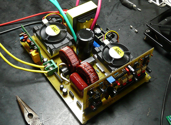
Pre-amp driver board
Empty board:
Installed as shown below:
Power-amp driver board
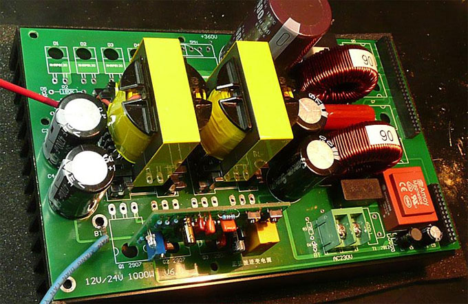
Power Board
Empty board:
PCB:
Installed as shown below:
Then, is the testing of the over-voltage protection. This part should not be difficult, there is not much to say (in accordance with the parameters of the drawings should be no problem).
Finally, is the most important test of overload and short circuit protection, and this is the most important property for an inverter.
Everything has been basically successful commissioning, load the 12V 300W Uni-polar Isolation Pure Sine Wave Inverter for more than one hour operating, and then shut down, discharge the high-voltage.
And then install the radiator, as it shown like this:
Want to buy one prototype. Please help.
Post a Comment:
You may also like:

Power Inverter Source
Featured Articles
How to Choose a Suitable Power ...
 How to select the inverter for an air conditioner, television, computer or the motor? How to match the battery? How long is the ...
How to select the inverter for an air conditioner, television, computer or the motor? How to match the battery? How long is the ...12V 300W Uni-polar Isolation Pure Sine ...
12v 300w uni-polar isolation of pure sine wave inverter Basic parameters Nominal power: 300W; continuous power: 250W; Peak power: ...
12v 300w uni-polar isolation of pure sine wave inverter Basic parameters Nominal power: 300W; continuous power: 250W; Peak power: ...600w Pure Sine Wave Power Inverter ...
 I spent nearly a month design a 600w pure sine wave power inverter. The machine has the following characteristics: 1. SPWM drive ...
I spent nearly a month design a 600w pure sine wave power inverter. The machine has the following characteristics: 1. SPWM drive ...1000w 12V DC Home Power Inverter ...
 This power inverter is designed for 12v DC, but also can be connected to 24v DC, my goal is 800 watt, strive to 1000 watt pure ...
This power inverter is designed for 12v DC, but also can be connected to 24v DC, my goal is 800 watt, strive to 1000 watt pure ...
Thanks