3000W Pure Sine Wave Inverter Design Report
I. Basic parameters

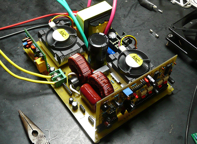
II. Basic situation of the inverter (architecture, composition)
All in all, says this is a 24V pure sine wave inverter, this power inverter is composed of three parts: 1. Front-driver board; 2. Stage drive plate; 3. Power board.
1. Pre-driver board
A. Auxiliary power supply
Function of the circuit is to power 24V battery voltage drops to about 13-15V and then through the LM7812 stable power supply to the control section 12V supply after the whole circuit, the first on the image:

In this circuit, BT input voltage range up to 15-36V, and the output stability in 12V. Q1 can also use the P-type MOS transistor, the appropriate selection of different types of P tube voltage can be done about 60V.
Below is concerned about the working principle of this circuit, the circuit starting moment, power is supplied through R21 sufficient base current, Q1 saturated conduction, its collector current through a portion of the charge supplied to the load L1 to C1,21 part is stored in L1 in. When the voltage exceeds 15V C21 ends when Q4 is turned on, Q3 is also turned cause the base potential of Q1 rises, current decreases, the potential of the upper end of the C12 decreases, since the voltage at both ends of the C12 cannot be mutated, the potential of the base of Q3 continues apace decreased base potential of Q1 rises rapidly until the fast turn-off, Q1 turns off, L1 stored energy is released through the freewheeling diode D7 to the C15 and the load, and then start the next cycle.
B. PWM driving portion
This is a SG3525 and professional MOS driver TC4452 driving ability of a drive circuit, TC4452 driving ability and reaction time are quite amazing, the internal integration MOS totem. The driving capacity can reach 13A.

When this part of the circuit access 12V power supply, SG3525 was electric, and then set up by the internal oscillator and external oscillator capacitor C11 and resistors R6 dead-time resistor R17 oscillation circuit generates huge tooth wave to provide a clock source for the entire IC, let IC work state, because access to the boot soft-start capacitor C14, a rectangular pulse is output after power changes start with the minimum duty cycle to 50% of the state, mainly to protect the signal driven MOS is not a boot step work in the larger duty cycle state to reduce the power-MOS moment of impact pressure.
Look SG3525, its PWM output is 11 feet and 14 feet and the feet of the output waveform 180 degrees out of phase, it is out of phase. After the two-way signal outputs respectively connected TC4452 PWM signal input side of the emitter follower is amplified by two current limiting resistors R16 and R18, the introduction of TC4452 before we see the two 10K resistors, respectively, of the PWM signal to ground. This drop has two functions, one to the SG3525 PWM signal plus a dummy load, so that the signal is not stable floating jump, the second is in the closed section of the inverter control switch signal input terminal TC4452 can have a stable low, the TC4452 will not some dry and produce a high level at the time of shutdown, the MOS gate of the power board while generating a high level, in the high-capacity battery power is turned on while the bombing.
When this part of the circuit SG3525 application that uses shallow closed loop modulation, the principle is to SG3525 2 feet of introducing a fixed reference, it is now 5V (produced by SG3525 16 feet), pin 1 to pre-boosted high pressure components, when the fixed value of the output high voltage component is greater than 2 feet, SG3525 error amplifier will be greater than the voltage variable 2 feet as an error, it amplifies the error amplified amount of the duty cycle of the PWM modulation, the inverter has a small quiescent current at no-load power. This feature is good in principle. Enable the PWM duty cycle at no load to a minimum, at the time of the tape should be immediately pulled the maximum duty cycle, using a circuit work at the highest efficiency state.
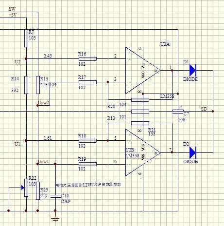
VI. Protection function
Protection part of the circuit as follows:

This circuit is a typical non-isolated inverter protection circuit that includes under-voltage protection, overcurrent protection, short circuit protection, thermal protection and the protection of self-locking.
Overload protection: non-isolated inverter overload mostly in H-bridge power stage under the S pole tube to the sampling resistor in series between the power ground, when there is an overload, there will be a large current flows through the sampling resistor and, thus, drop, a professional comparator this voltage drop and collect a fixed threshold into it compared to some value greater than the output high, then cited the high level to do to protect shutdown signal, when the overload shutdown and PWM SPWM drive signal protection MOS not hang because of excessive current.
Short circuit protection: In a similar figure, short circuit protection and overload protection mode, short circuit protection is a serious overload, overload only constant RC delay to be set after a short circuit in the post-stage H-bridge MOS does not burn in the range can be.
Overheat protection: This protection is single room, a basic level of theory, R14, R15 6V voltage obtained by dividing the inverting input of the comparator as a threshold value, the positive phase ends with the same thermal RT and R13 form a voltage divider, when the temperature reaches 65 degrees when the partial pressure just to 6V, the comparator output is high, the signal can be incorporated to protect.
Protection Self-locking: I will be designed with self-locking and under-voltage. In this 3000W inverter, I over-voltage level is not the first to do so here for setting under-voltage of R30, R37, and not soldered on the board, drawn mainly want to use this in a single driver board when under-voltage protection may be provided. Substituted R30 and R37 and R28 are 6V regulator, the LM339 to 6 feet for a 6V it’s prospective. This role is, first, a threshold to 6 feet, and the other is 6-pin voltage clamp, use the machine in an instant with a large load was allowed by the impact.
Self-locking principle: When overload, short circuit or overheating of any one comparator protective signals are respectively through D5, D2, D6 a high level of about 11V closed to LM339 5 feet, 5 feet voltage is greater than 6 feet voltage, the comparator inverting output high, and this high level D3 received by 5 feet, 5 feet 6 feet has been greater than this comparator has output high! Always shut off the PWM and SPWM, stop the inverter, safe and effective protection MOS power tube!
Here is the application of LM339, each input pin must be connected to a capacitor of about 103. The output pin must have a pull-up resistor 1K-3K. In addition, if the inverting terminal as a reference, it should be given a high level preset at boot time, you can effectively avoid a boot is a comparator output is high, resulting in a boot to protect the machine!
RC dead-band setting: In order not to make the H-bridge with a total edge guide, to set appropriate SPWM dead zone is necessary.
Simply put under RC dead-band how such hardware is implemented to IC3C here as an example: SPWM actually microcontroller according to a certain algorithm DA converter out of the price ladder wave, that it is still a switching signal to a switch signal analyze it, at a high level, all the way to the door and received 8 feet, another way to C17 charge through R19, C17 charge in the unfinished stage, 9 feet where the signal is "0", then the and gate output is low, when C17 after charging is completed, only 9 feet to "1" and the output signal can be synthesized gate, then the middle on a charge time interval R19 to C17, and this time is what we call dead time.
IR2110 driver circuit is a typical application circuit, did not join the negative pressure, because some non-isolated inverter section of the machine, do the negative pressure, not so good to do, but also no too hard, but you can rest assured that work perfectly normal.
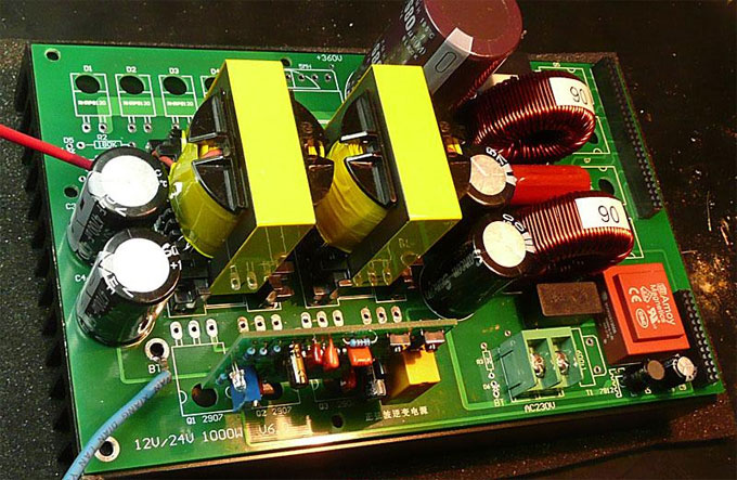
V. Power board
Power board frontstage uses eight IC4025 main transformers, 16 sets of 190N08. The backstage uses 4 sets of N FQL40N50 pipe. But four sets can only offer low power, if we want more we can buy large 120N50, 120A500V MOS. The power will be stronger, but the price will also be higher. In addition the machine is bipolar modulation, to a 47 sendust, 60U-90U ring do 1.5UH output filter inductor.
- Nominal power 3000W
- Continuous power; 2800W
- 6000W peak power
- Overall efficiency: >87%
- Overload protection: 3200W 3S
- Voltage protection: 20V 5S delay shutdown, overvoltage protection 30V immediate shutdown
- Overheat protection: 65 degrees
II. Basic situation of the inverter (architecture, composition)
All in all, says this is a 24V pure sine wave inverter, this power inverter is composed of three parts: 1. Front-driver board; 2. Stage drive plate; 3. Power board.
- Pre-driver board is mainly made up of three small parts, an auxiliary power supply section, a part of the PWM drive, and the third part is the protection portion;
- After the class driver board consists of three parts, one is to generate SPWM signals (MCU to complete) section, a hardware RC dead time setting section; then one is driving portion of the IR2110.
- The power board consists of four main parts, one is the pre-booster and rectifier filter, and the second part is a full-bridge sine transformation stage H, the third part is the regulator feedback; fourth is the LC filter section.
1. Pre-driver board
A. Auxiliary power supply
Function of the circuit is to power 24V battery voltage drops to about 13-15V and then through the LM7812 stable power supply to the control section 12V supply after the whole circuit, the first on the image:
In this circuit, BT input voltage range up to 15-36V, and the output stability in 12V. Q1 can also use the P-type MOS transistor, the appropriate selection of different types of P tube voltage can be done about 60V.
Below is concerned about the working principle of this circuit, the circuit starting moment, power is supplied through R21 sufficient base current, Q1 saturated conduction, its collector current through a portion of the charge supplied to the load L1 to C1,21 part is stored in L1 in. When the voltage exceeds 15V C21 ends when Q4 is turned on, Q3 is also turned cause the base potential of Q1 rises, current decreases, the potential of the upper end of the C12 decreases, since the voltage at both ends of the C12 cannot be mutated, the potential of the base of Q3 continues apace decreased base potential of Q1 rises rapidly until the fast turn-off, Q1 turns off, L1 stored energy is released through the freewheeling diode D7 to the C15 and the load, and then start the next cycle.
B. PWM driving portion
This is a SG3525 and professional MOS driver TC4452 driving ability of a drive circuit, TC4452 driving ability and reaction time are quite amazing, the internal integration MOS totem. The driving capacity can reach 13A.
When this part of the circuit access 12V power supply, SG3525 was electric, and then set up by the internal oscillator and external oscillator capacitor C11 and resistors R6 dead-time resistor R17 oscillation circuit generates huge tooth wave to provide a clock source for the entire IC, let IC work state, because access to the boot soft-start capacitor C14, a rectangular pulse is output after power changes start with the minimum duty cycle to 50% of the state, mainly to protect the signal driven MOS is not a boot step work in the larger duty cycle state to reduce the power-MOS moment of impact pressure.
Look SG3525, its PWM output is 11 feet and 14 feet and the feet of the output waveform 180 degrees out of phase, it is out of phase. After the two-way signal outputs respectively connected TC4452 PWM signal input side of the emitter follower is amplified by two current limiting resistors R16 and R18, the introduction of TC4452 before we see the two 10K resistors, respectively, of the PWM signal to ground. This drop has two functions, one to the SG3525 PWM signal plus a dummy load, so that the signal is not stable floating jump, the second is in the closed section of the inverter control switch signal input terminal TC4452 can have a stable low, the TC4452 will not some dry and produce a high level at the time of shutdown, the MOS gate of the power board while generating a high level, in the high-capacity battery power is turned on while the bombing.
When this part of the circuit SG3525 application that uses shallow closed loop modulation, the principle is to SG3525 2 feet of introducing a fixed reference, it is now 5V (produced by SG3525 16 feet), pin 1 to pre-boosted high pressure components, when the fixed value of the output high voltage component is greater than 2 feet, SG3525 error amplifier will be greater than the voltage variable 2 feet as an error, it amplifies the error amplified amount of the duty cycle of the PWM modulation, the inverter has a small quiescent current at no-load power. This feature is good in principle. Enable the PWM duty cycle at no load to a minimum, at the time of the tape should be immediately pulled the maximum duty cycle, using a circuit work at the highest efficiency state.
VI. Protection function
Protection part of the circuit as follows:
This circuit is a typical non-isolated inverter protection circuit that includes under-voltage protection, overcurrent protection, short circuit protection, thermal protection and the protection of self-locking.
Overload protection: non-isolated inverter overload mostly in H-bridge power stage under the S pole tube to the sampling resistor in series between the power ground, when there is an overload, there will be a large current flows through the sampling resistor and, thus, drop, a professional comparator this voltage drop and collect a fixed threshold into it compared to some value greater than the output high, then cited the high level to do to protect shutdown signal, when the overload shutdown and PWM SPWM drive signal protection MOS not hang because of excessive current.
Short circuit protection: In a similar figure, short circuit protection and overload protection mode, short circuit protection is a serious overload, overload only constant RC delay to be set after a short circuit in the post-stage H-bridge MOS does not burn in the range can be.
Overheat protection: This protection is single room, a basic level of theory, R14, R15 6V voltage obtained by dividing the inverting input of the comparator as a threshold value, the positive phase ends with the same thermal RT and R13 form a voltage divider, when the temperature reaches 65 degrees when the partial pressure just to 6V, the comparator output is high, the signal can be incorporated to protect.
Protection Self-locking: I will be designed with self-locking and under-voltage. In this 3000W inverter, I over-voltage level is not the first to do so here for setting under-voltage of R30, R37, and not soldered on the board, drawn mainly want to use this in a single driver board when under-voltage protection may be provided. Substituted R30 and R37 and R28 are 6V regulator, the LM339 to 6 feet for a 6V it’s prospective. This role is, first, a threshold to 6 feet, and the other is 6-pin voltage clamp, use the machine in an instant with a large load was allowed by the impact.
Self-locking principle: When overload, short circuit or overheating of any one comparator protective signals are respectively through D5, D2, D6 a high level of about 11V closed to LM339 5 feet, 5 feet voltage is greater than 6 feet voltage, the comparator inverting output high, and this high level D3 received by 5 feet, 5 feet 6 feet has been greater than this comparator has output high! Always shut off the PWM and SPWM, stop the inverter, safe and effective protection MOS power tube!
Here is the application of LM339, each input pin must be connected to a capacitor of about 103. The output pin must have a pull-up resistor 1K-3K. In addition, if the inverting terminal as a reference, it should be given a high level preset at boot time, you can effectively avoid a boot is a comparator output is high, resulting in a boot to protect the machine!
RC dead-band setting: In order not to make the H-bridge with a total edge guide, to set appropriate SPWM dead zone is necessary.
Simply put under RC dead-band how such hardware is implemented to IC3C here as an example: SPWM actually microcontroller according to a certain algorithm DA converter out of the price ladder wave, that it is still a switching signal to a switch signal analyze it, at a high level, all the way to the door and received 8 feet, another way to C17 charge through R19, C17 charge in the unfinished stage, 9 feet where the signal is "0", then the and gate output is low, when C17 after charging is completed, only 9 feet to "1" and the output signal can be synthesized gate, then the middle on a charge time interval R19 to C17, and this time is what we call dead time.
IR2110 driver circuit is a typical application circuit, did not join the negative pressure, because some non-isolated inverter section of the machine, do the negative pressure, not so good to do, but also no too hard, but you can rest assured that work perfectly normal.
V. Power board
Power board frontstage uses eight IC4025 main transformers, 16 sets of 190N08. The backstage uses 4 sets of N FQL40N50 pipe. But four sets can only offer low power, if we want more we can buy large 120N50, 120A500V MOS. The power will be stronger, but the price will also be higher. In addition the machine is bipolar modulation, to a 47 sendust, 60U-90U ring do 1.5UH output filter inductor.
Post a Comment:
You may also like:

Power Inverter Source
Featured Articles
How to Choose a Suitable Power ...
 How to select the inverter for an air conditioner, television, computer or the motor? How to match the battery? How long is the ...
How to select the inverter for an air conditioner, television, computer or the motor? How to match the battery? How long is the ...12V 300W Uni-polar Isolation Pure Sine ...
 12v 300w uni-polar isolation of pure sine wave inverter Basic parameters Nominal power: 300W; continuous power: 250W; Peak power: ...
12v 300w uni-polar isolation of pure sine wave inverter Basic parameters Nominal power: 300W; continuous power: 250W; Peak power: ...600w Pure Sine Wave Power Inverter ...
 I spent nearly a month design a 600w pure sine wave power inverter. The machine has the following characteristics: 1. SPWM drive ...
I spent nearly a month design a 600w pure sine wave power inverter. The machine has the following characteristics: 1. SPWM drive ...1000w 12V DC Home Power Inverter ...
 This power inverter is designed for 12v DC, but also can be connected to 24v DC, my goal is 800 watt, strive to 1000 watt pure ...
This power inverter is designed for 12v DC, but also can be connected to 24v DC, my goal is 800 watt, strive to 1000 watt pure ...
And more light on that errow amplifier
Ugochukwujonathan@gmail.com